


|
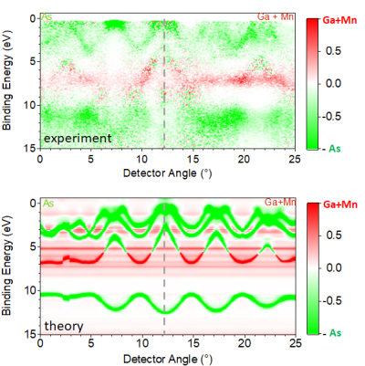
The dilute magnetic semiconductors have promise in spin-based electronics applications due to their potential for ferromagnetic order at room temperature, and various unique switching and spin-dependent conductivity properties. However, the precise mechanism by which the transition-metal doping produces ferromagnetism has been controversial. We have studied a dilute magnetic semiconductor (5% manganese-doped gallium arsenide) with
Bragg-reflection standing-wave hard X-ray angle-resolved photoemission spectroscopy, and
resolved its electronic structure into element- and momentum- resolved components. The
measured valence band intensities have been projected into element-resolved components
using X-ray standing-wave technique, with results in excellent agreement with element-projected Bloch spectral functions and clarification of the electronic structure of this prototypical material.
Nemšák et al., Nature Communications 9 (2018) Highlight on phys.org |
|
|
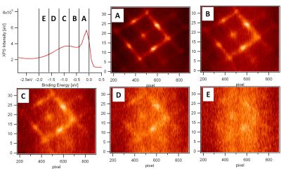
Low-energy electron microscopy, micro-electron diffraction, X-ray absorption spectroscopy, and photoemission electron microscopy create a powerful collection of techniques that were used to determine the morphology, shape, chemical state, and crystal structure of the ceria nanoislands grown on single-crystalline substrates. Utilizing real-time observation capabilities, we revealed a three-way interaction between the ceria, substrate, and local oxygen chemical potential, which determines the shape and the growth mode of the islands. Last, but not least, we pointed out the influence of crystal imperfections, which can heavily influence the redox properties of model systems and which have to be studied on the microscopic level. The awareness of the surface science community about presence of such defects was hopefully raised.
Hackl, Nemšák et al., Surface Science (2018) Hackl, Nemšák et al., Ultramicroscopy (2017) |

|
|
Studies of the electrified solid–liquid interfaces are crucial for understanding biological and electrochemical systems. Until recently, use of photoemission electron microscopy (PEEM) for such purposes has been hampered by incompatibility of the liquid samples with ultrahigh vacuum environment of the electron optics and detector. Here we demonstrate that the use of ultrathin electron transparent graphene membranes, which can sustain large pressure differentials and act as a working electrode, makes it possible to probe electrochemical reactions in operando in liquid environments with PEEM.
Nemšák et al., Topics in Catalysis (2018) Nemšák et al., Journal of American Chemical Society (2017) |

|
|
Complex oxides and their interfaces are of great interest and importance for next generation
applications in electronics and spintronics. The shining example is a GTO/STO system, which
is known to exhibit interfacial conductivity despite the fact, that both oxides are insulators.
Angle-resolved photoelectron spectroscopy was used for a direct mapping of occupied electron states
in the proximity of Fermi edge and a 2D electron gas was observed. A depth resolution of a standard
XPS was enhanced by using a standing-wave approach, which was needed to prove that the origin of
observed electronic structure lies within the GTO/STO interface.
Nemšák et al., Physical Review B (2016) Nemšák et al., Applied Physics Letters (2015) |
|
|
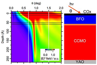
The electric field control of functional properties is a crucial goal in oxide-based electronics. Nonvolatile switching between different resistivity or magnetic states in an oxide channel can be achieved through charge accumulation or depletion from an adjacent ferroelectric. However, the way in which charge distributes near the interface between the ferroelectric and the oxide remains poorly known, which limits our understanding of such switching effects. Here, we use a first-of-a-kind combination of scanning transmission electron microscopy with electron energy loss spectroscopy, near-total-reflection hard X-ray photoemission spectroscopy, and ab initio theory to address this issue. We achieve a direct, quantitative, atomic-scale characterization of the polarization-induced charge density changes at the interface between the ferroelectric BiFeO3 and the doped Mott insulator Ca1–xCexMnO3, thus providing insight on how interface-engineering can enhance these switching effects.
Marinova, Nemšák et al., Nano Letters (2015) |
|
|
Heterogeneous processes at solid/gas, liquid/gas and solid/liquid interfaces are ubiquitous in
modern devices and technologies but often difficult to study quantitatively. Full characterization
requires measuring the depth profiles of chemical composition and state with
enhanced sensitivity to narrow interfacial regions of a few to several nm in extent over those
originating from the bulk phases on either side of the interface. We show for a model system
of NaOH and CsOH in an ~1-nm thick hydrated layer on alpha-Fe2O3 (haematite) that combining
ambient-pressure X-ray photoelectron spectroscopy and standing-wave photoemission
spectroscopy provides the spatial arrangement of the bulk and interface chemical species, as
well as local potential energy variations, along the direction perpendicular to the interface
with sub-nm accuracy. Standing-wave ambient-pressure photoemission spectroscopy is thus
a very promising technique for measuring such important interfaces, with relevance to energy
research, heterogeneous catalysis, electrochemistry, and atmospheric and environmental
science.
Nemšák et al., Nature Communications (2014) |

|
|
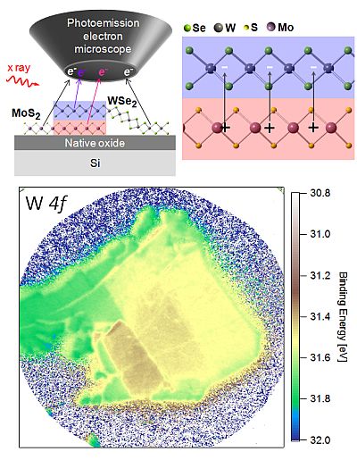
Since their invention, semiconductor heterostructures have been the fundamental platform for many important
applications such as lasers, light-emitting diodes, solar cells, and high-electron-mobility transistors1. Analogous
to the traditional heterostructures, layered transition metal dichalcogenide (TMDC) heterostructures can be designed
and built by assembling individual single layers into functional multilayer structures, but in principle with atomically
sharp interfaces, no interdiffusion of atoms, digitally controlled layered components and no lattice parameter constraints.
The optoelectronic behavior of this new type of van der Waals semiconductor heterostructure, however, remains still unknown
at the single layer limit. Here we investigate artificial semiconductor heterostructures built from single layer WSe2 and MoS2
building blocks. We observe a strong interlayer interaction manifested by ~400 mV built-in potential between the two single layer
components as measured by x-ray photoelectron microscopy. A large Stokes-like shift of ~100 meV between the photoluminescence peak
and the lowest absorption peak is observed which is consistent with a type II band alignment with spatially indirect emission. We further
observe strong photoluminescence from the WSe2/MoS2 hetero-bilayer, much stronger than from the corresponding homo-bilayers, indicating
a direct transition in reciprocal space. W 4f7/2 binding energy position contour plot of the sample is shown on the right.
Hui, Nemšák et al., Proceedings of National Academy of Sciences (2014) |
|
|
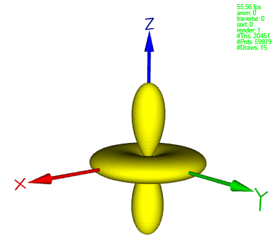
Based on a paper by Goldberg et al, a web-based user interface for calculating and plotting spatially resolved photoionization cross-section is under development and will be deployed for general use. An example on right is a preview showing O 2pz orbital photoelectron cross-section for 5000 eV excitation with a polarization vector parallel to [001].
Goldberg et al., Journal of Electron Spectroscopy (1985) Nemšák et al., in preparation |
|
|
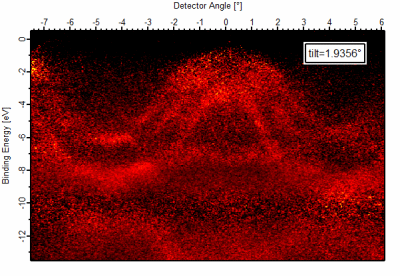
Hard X-ray excitation in Photoelectron Spectroscopy brings huge benefits in terms of information depth, which is crucial
for probing buried interfaces as well as for supressing the influence of surface, when information about bulk is needed.
Valence band structure of W(110) was observed along [001] direction using 2.5 keV primary light at BL9.3.1, Advanced Light
Source. A rotatable chamber equipped with upgraded Scienta SES-2002 analyzer was used to collect the data. The chamber rotation
and data stitching was needed to obtain the presented figure.
Fadley, Nemšák, Journal of Electron Spectroscopy (2014) |
|
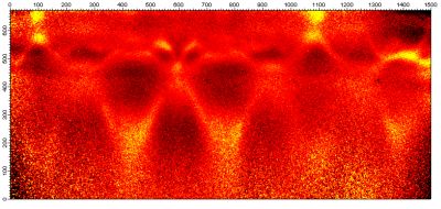
| Despite huge advantages of angle-resolved photoelectron spectroscopy in hard X-rays regime (increased probing depth), the technique battles a disfavor of photoelectron cross-section drop as well as increased phonon effects. In order to obtain a full 3D data set of k|| vs. E plots, an analyzer with high angular resolution and a six axes manipulator is needed for efficient scanning through the Brillouin zones. Valence band structure of SiC(0001) was measured in full 2D fashion with 3.1 keV primary light at BL9.3.1, Advanced Light Source. Scienta SES-2002 analyzer with upgraded lens tables (angular resolution better than 0.1 degree) was used to collect the data. |
|
|
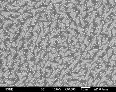
Thin oxide layers grown on metal surfaces have attracted a lot of attention in surface science over the last two decades. Interest has been stimulated not only by their prospective use in electronic and magneto-electronic devices, but also because of their role in surface science as model counterparts to bulk oxide substrates. Such ultra-thin layers do not suffer from charging effects and are perfect candidates for chemically inert substrates in model catalyst photoelectron spectroscopy studies. Epitaxial thin alumina layers are usually grown by oxidation of single-crystalline aluminum-containing alloy samples. The phenomenon of surface segregation of aluminum atoms at elevated temperatures is used as a supply mechanism of aluminum in order to form alumina films.
We've prepared epitaxial ultra-thin alumina layers on a wide range of substrates - from Ni-Al and Cu-Al alloys to Cu, Co and Ni single-crystalline substrates. Figure depicts SEM image demonstrating the morphology of such layer grown on a Cu(111) substrate. Nemšák et al., Journal of Physics: Condensed Matter (2013) Nemšák et al., Surface Science (2010) Nemšák et al., Surface and Interface Analysis (2010) |
|
|
Bimetallic systems attract a great deal of interest due to their unique properties, which are results of the mutual bonding and the changes in the electronic structure. Strong effects are observed for bimetallic systems that combine metals with an electron-rich d-band (late transition metal) and metals with an electron-poor valence band (early-transition
or sp metal). Transition metals like Pd are widely used as a catalyst in a number of oxidation reactions, especially hydrocarbon and CO oxidation in automotive exhaust and industry.
The XPS (X-ray Photoelectron Spectroscopy) investigation of Pd–Sn alloy indicated a strong bimetallic interaction resulting in a noble metal-like electronic structure. We've prepared a model Pd-Sn catalyst using molecular beam epitaxy and characterized the prepared nanoparticles by means of XPS and electron diffraction techniques. A core-shell structure made of Pd core and Pd-Sn shell was further investigated with respect to its catalytic properties. Figure shows the influence of CO adsorption/desorption on electronic state of Sn present in the shell of the nanoparticles. Nemšák et al., Surface Science (2008) |

|